

Sneak peek: Electronics Forge, from a written brief to a routed PCB

Hi everyone,
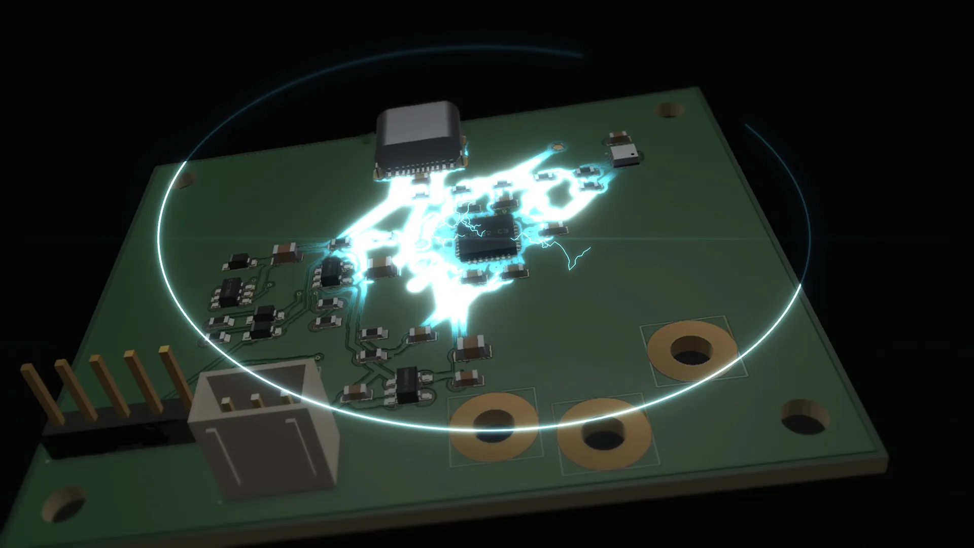
This is a first look at the Autonomous Electronics engineer.
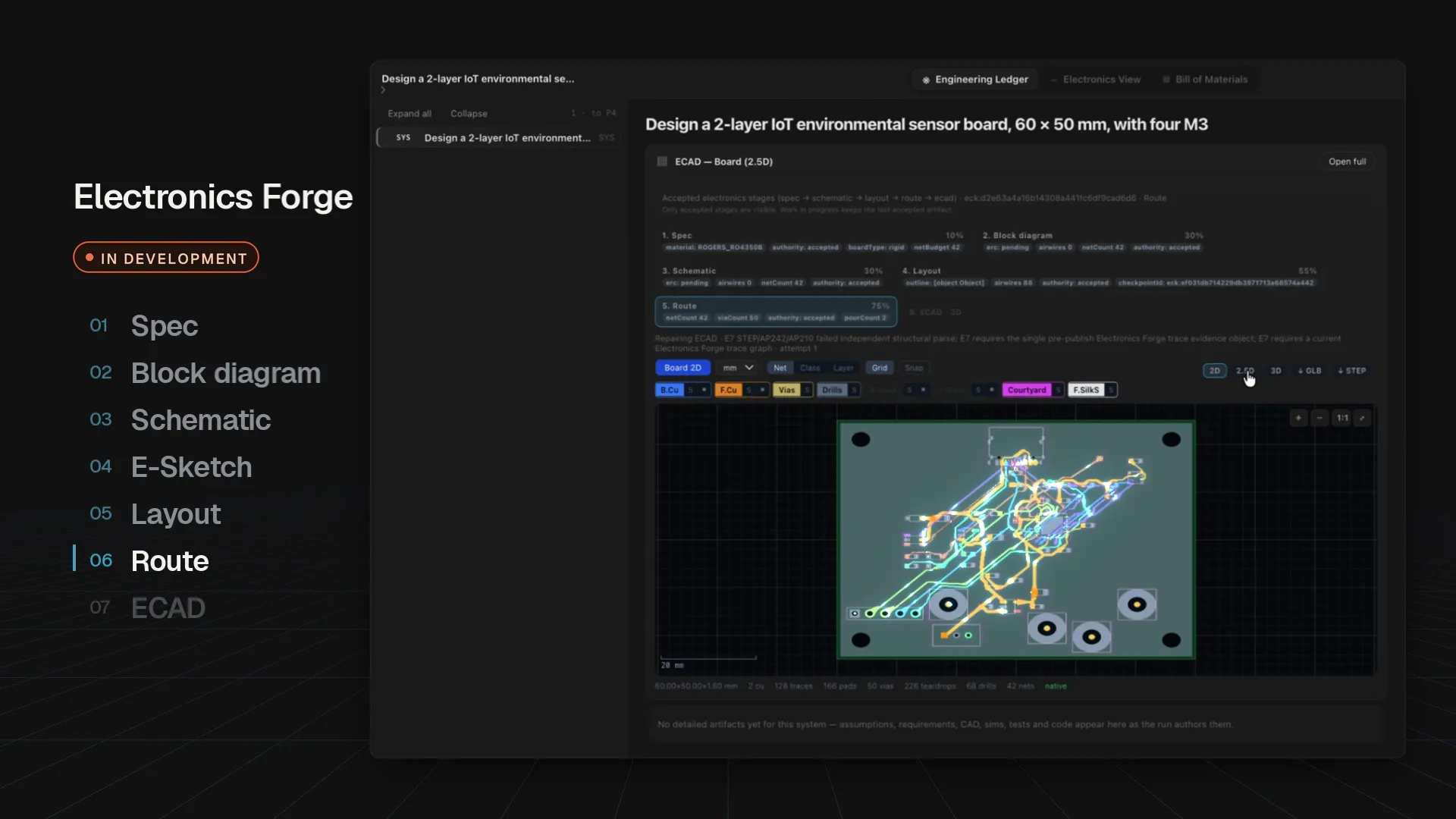
You give it a brief and it builds the board in stages: spec, block diagram, schematic, E-Sketch, layout, route, ECAD. Each stage is its own artifact you can open and inspect.
Our bold vision is for Everyone, regardless of their engineering know-how, to be able to create functional, manufacturable, multidisciplinary products using natural language - electronics, mechanical, controls and software/firmware. The same experience folks enjoy in tools like Lovable for vibe-coding, extended to complex, real-life systems.
We will continuously extend our part libraries for electronics and add specialized functions, like LED chip creation.
Soon we'll start a public PCB/chip library on our website, stay tuned.
What would you need to see before trusting a board you didn’t route yourself?
Replies
Going from a short brife to a full boards a jump. Would be nice to see how it control changes along the way.
@_gary_g That jump is exactly why it runs in stages. Spec, block diagram, schematic, E-Sketch, layout, route and ECAD are each a checkpoint that gets accepted, and while something is being reworked you keep seeing the last accepted version. We`d be happy to hear your feedback if you try it!
I like that you can chcek each step along the way. It makes thewhole process easier to follow.
@jadiwang Thank you, that was the whole idea. Every stage stays open to inspect, so you never end up with a board you can't trace back. If you try it on a project, tell us where it gets hard to follow.
looking amazing! one discipline after the other until complete, multidisciplinary products are created from one prompt 😀
i'd want to see the electrical rule checks and a way to test the design before sending it for manufacturing. A board can look fine on screen but still have issues in real life. Does Electronic Forge include any validation beyond routing?
@chritopher_bond Great point! Autonomyware understands engineering end to end. You can create your specifications and Autonomyware takes them into account while creating the 3D. Or let the AI create the entire product. Ultimately, the builder is always in control and does the final review and approval before a product is produced, the same way it is done today in engineering.
I'd want to see the DRC report, not just a pass/fail badge. Show me every clearance violation it suppressed or auto-fixed, and let me click through to the geometry it changed.
@chaity_okpalanozie Agreed, a badge without the list behind it proves nothing, especially when the tool fixes things on its own. Thank you for taking the time, we`ll be sure to implement these feedbacks, they are very useful to us.
Show me the stackup and impedance assumptions. What dielectric, what trace width for 50Ω, and did it actually verify impedance or just guess from a default stackup?
@sulemna_ola That's the line between engineering and guessing, which is why it helps that the stackup sits in the spec as an explicit requirement, not a default. On a 2-layer, 1.6 mm board like this one, would you accept a calculated impedance with every assumption shown, or only a field-solver result?
I need to see the return path. For every high-speed net, show me where the current actually returns, ground plane continuity, no splits under traces, no reference plane changes without stitching vias
@moses_habila On a 2-layer board that's the question that matters most. Return-path rules per net (plane continuity, no splits under traces, stitching wherever the reference changes) are exactly what we want the router to prove and show, not just follow quietly. Noted for the beta, and if you have a board that's tough on return paths, we'd like to run it through.
@theo_gzd Who's liable? If this board fails EMC or catches fire, is there an engineering sign-off, an insurance policy, or just a terms-of-service disclaimer?
@denizmilli06 Great question, thank you! It works like any CAD or ECAD tool: whoever releases the product signs it off, and EMC and safety certification still happen in a lab, as they should. What changes is everything before that point. Autonomyware engineers the board and keeps the evidence behind each decision, traced back to the requirements, so sign-off becomes a review rather than a redo. It will support the compliance work along the way too.
Give me the netlist diff. If the schematic changed during layout. Even a pin swap or a gate rename, I want a side-by-side of what the netlist was versus what got routed.
@nancy_philip Agreed, and pin swaps are the sneaky ones because they look harmless in layout. Every stage is already stored as its own versioned artifact, so comparing what the schematic said with what got routed is the natural check to expose. Would you want only the differences, or the full side-by-side every time?
Thermal. Where are the hot components, what's the copper area on those nets, and did it add thermal vias or just drop a pour and call it done?
@tomderaad05 good point! We are working on simulations as part of the roadmap in general. This does not just cover thermal simulation but also structural simulation, for example FEA for mechanical parts. Keep an eye out for our next release!